
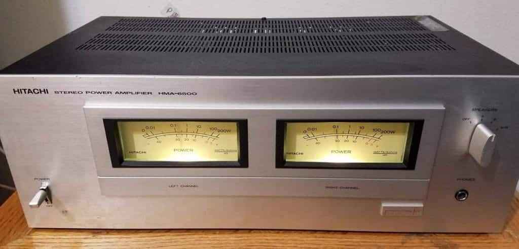
Hitachi HMA6500 ,little mosfet amp from Yore ….. resurrection , by ZM
Well , it started several months ago , few boyz at Baby Diyaudio asked for advice which second hand amp to buy . Some members started ( even if that’s really DIY forum) talking about synergy , lalala , blahblah …… while I remember seeing few interesting amps on local adds site , of which one is venerable and indefinitely cute little amp form Yore – Hitachi HMA6500.
Well – it’s hard to buy anything better for that sort of Eu greenies nowadays ….. around 100E .
I gave them my advice , also offering my help in rejuvenation and optional tweaking/changing circuit , in form of forum public correspondence .
However , one of boyz (asking for advice) really wasn’t too serious about thing (vanishing in mist of other (read – FiFi) local forums asking same question again and again) , while other member asking was serious but not so skilled in electronics, to be able to make necessary rejuve process by himself.
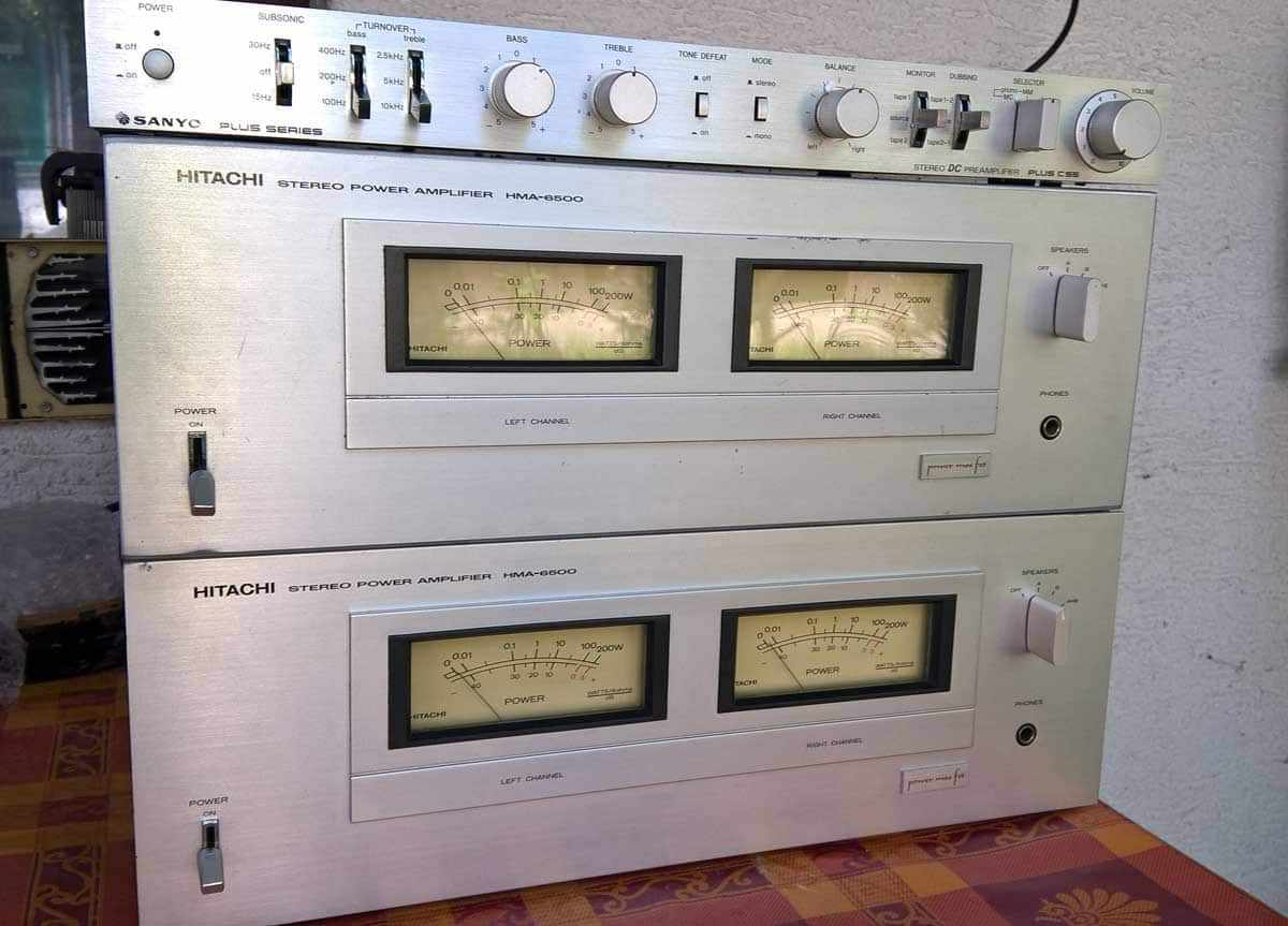
So …… few days later , two of them are acquired (one for (now) customer ,one for your truly …. to have around) , along with decent preamp to mate with .
Preamp will be , in few days , object of separate blog post .
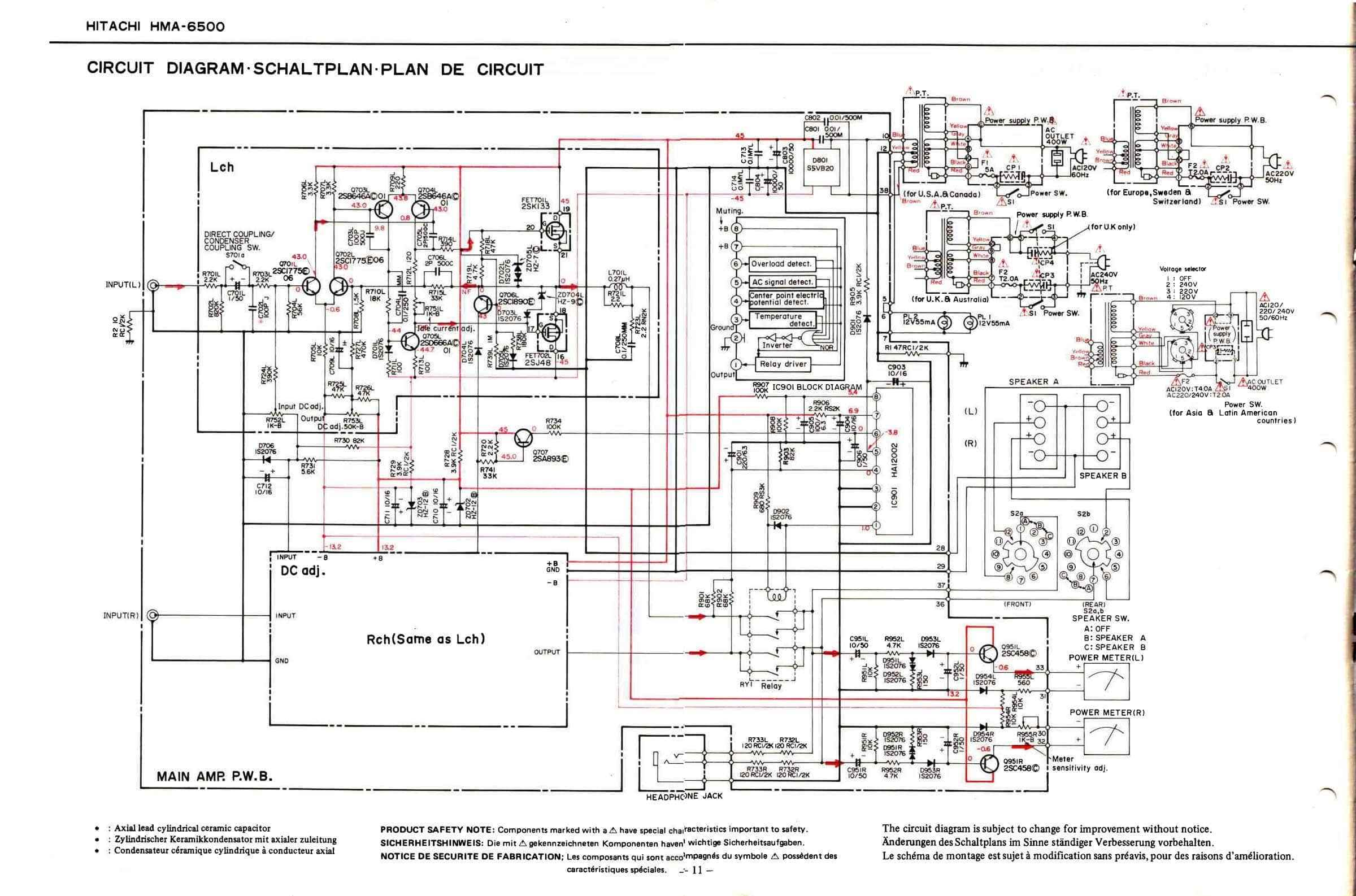
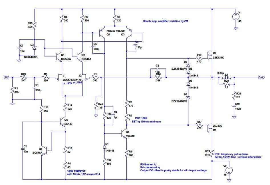
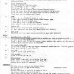
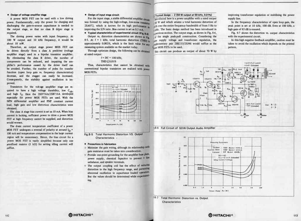
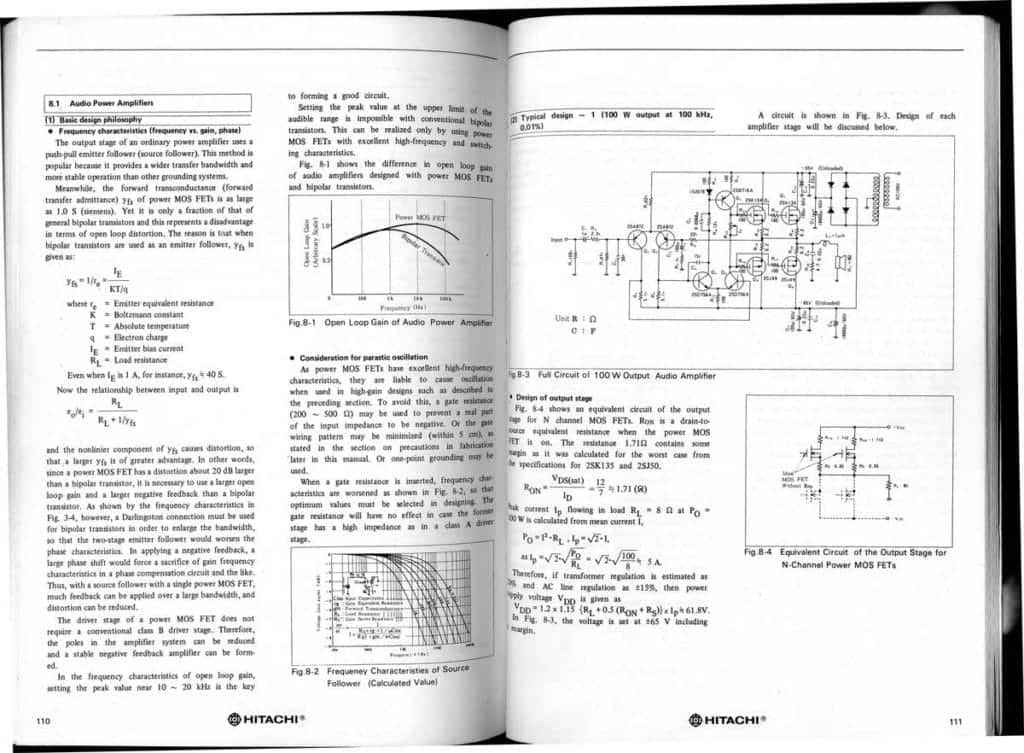
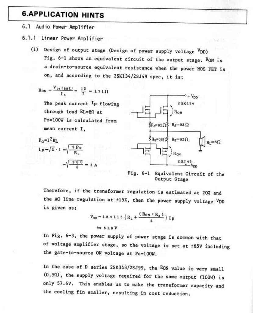
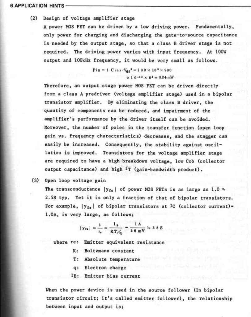
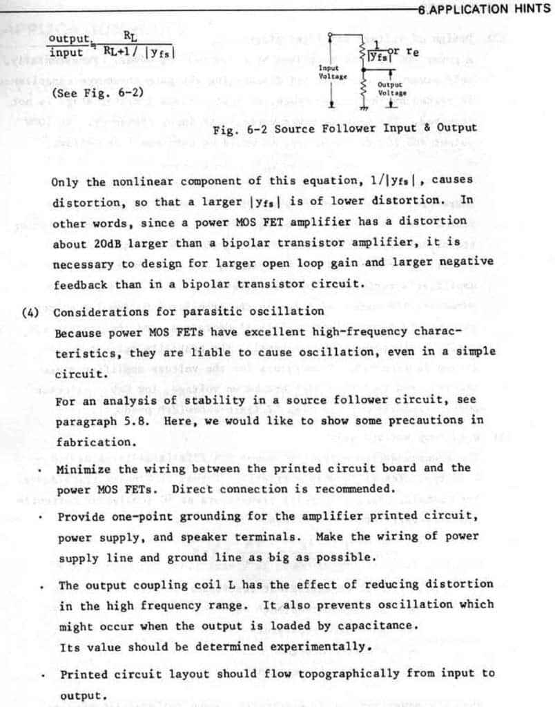
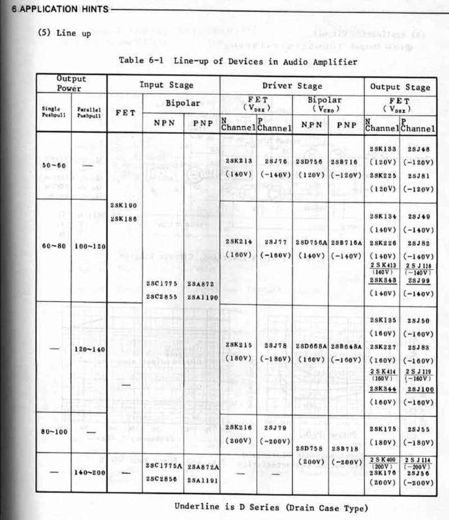
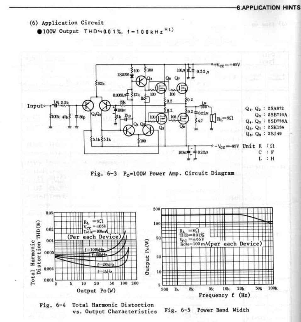
Now , little history lesson , old Hitachi papers , written when Hitachi Mosfets were latest and newest bling :
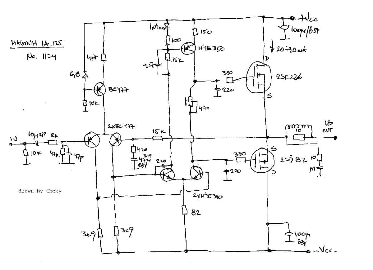
Not small number of amps was made by these basic schematic , and one of them was Magnum IA125 , integrated amplifier made by small England Manufacture , which I had eons ago , now happily making music in home of my good Pal’s bro ……..
Observe miniscule Iq …… that was British fashion these days …. 🙂
 So , amp is cute , good tweaking potential , cheap to buy and improve .
Here is factory schematic :
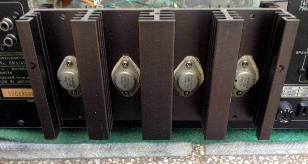
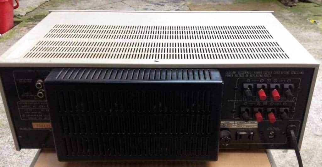
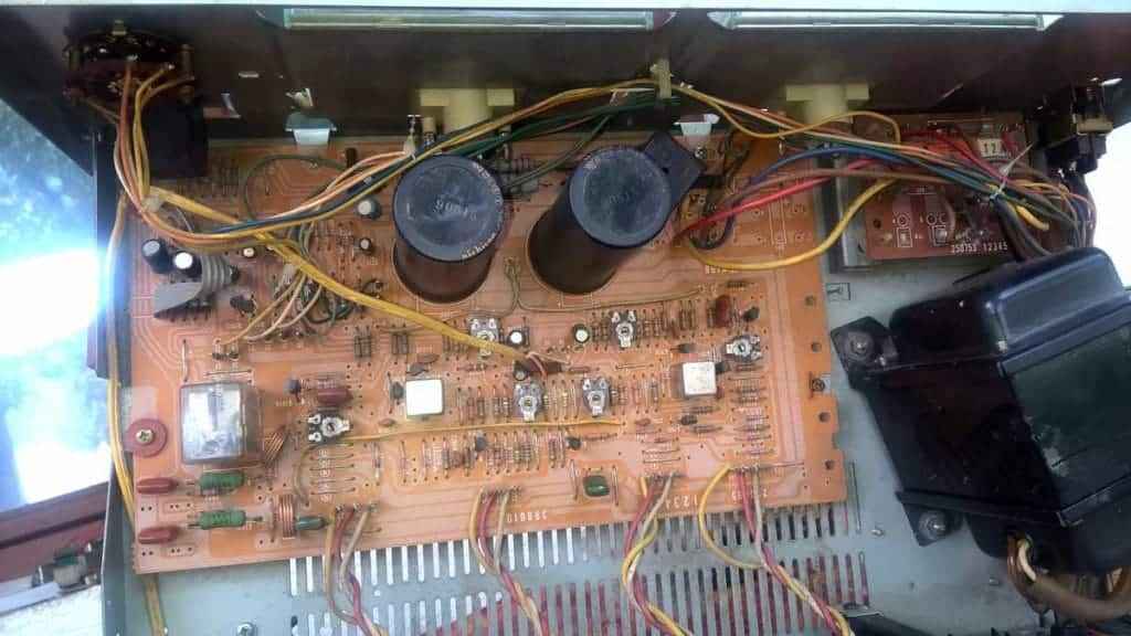
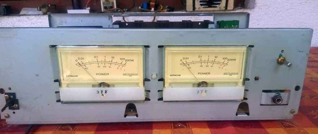
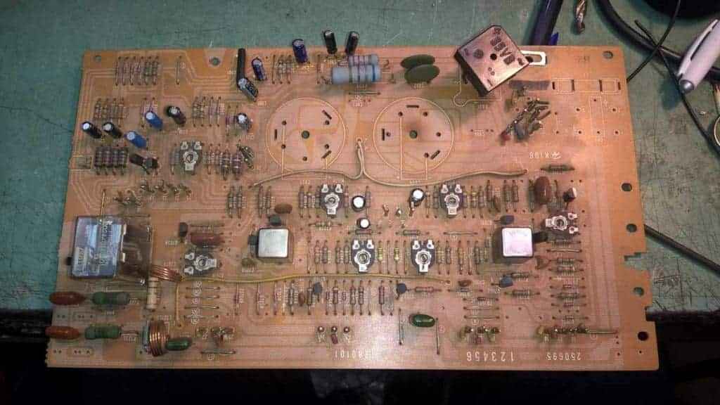
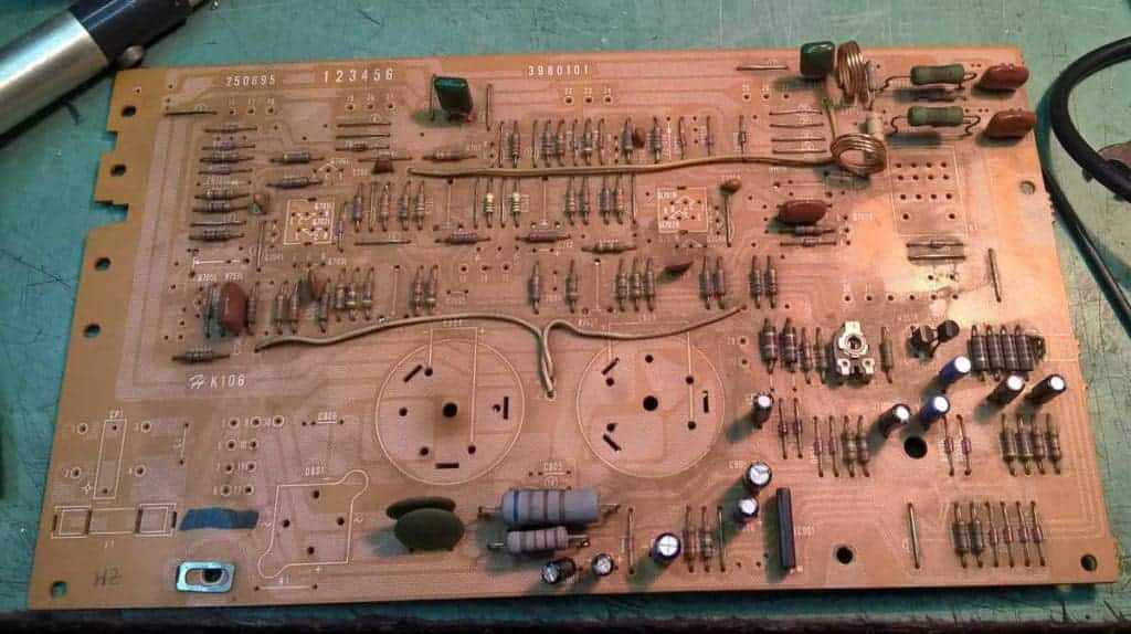
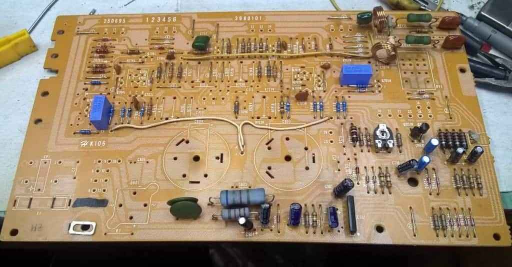
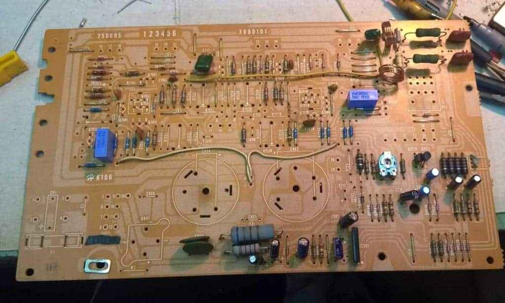
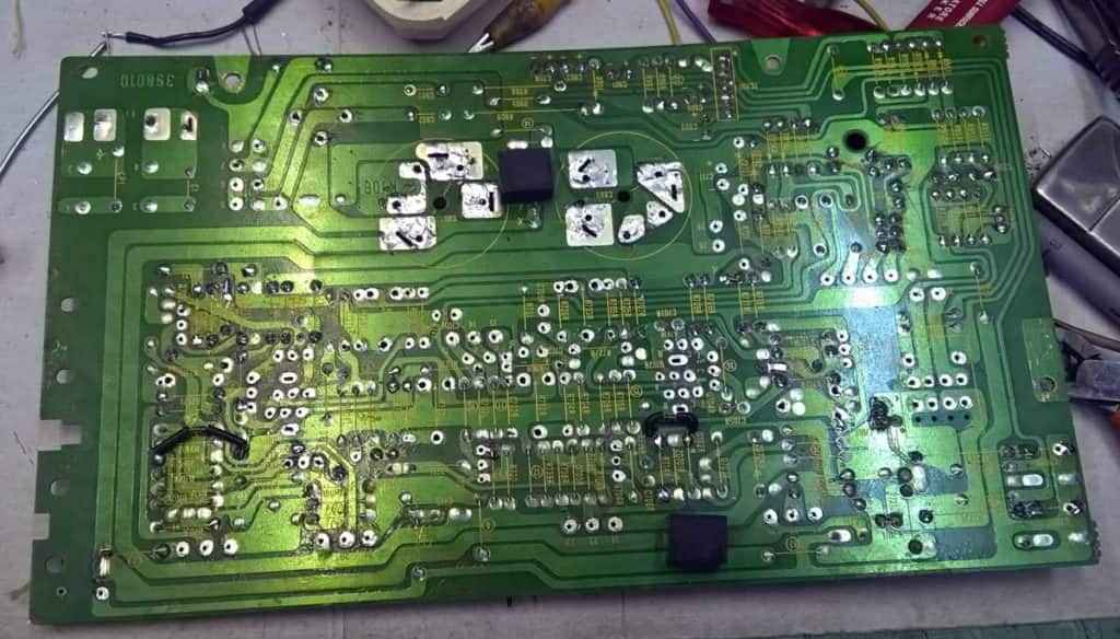
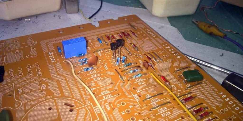
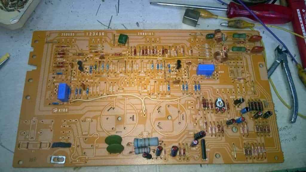
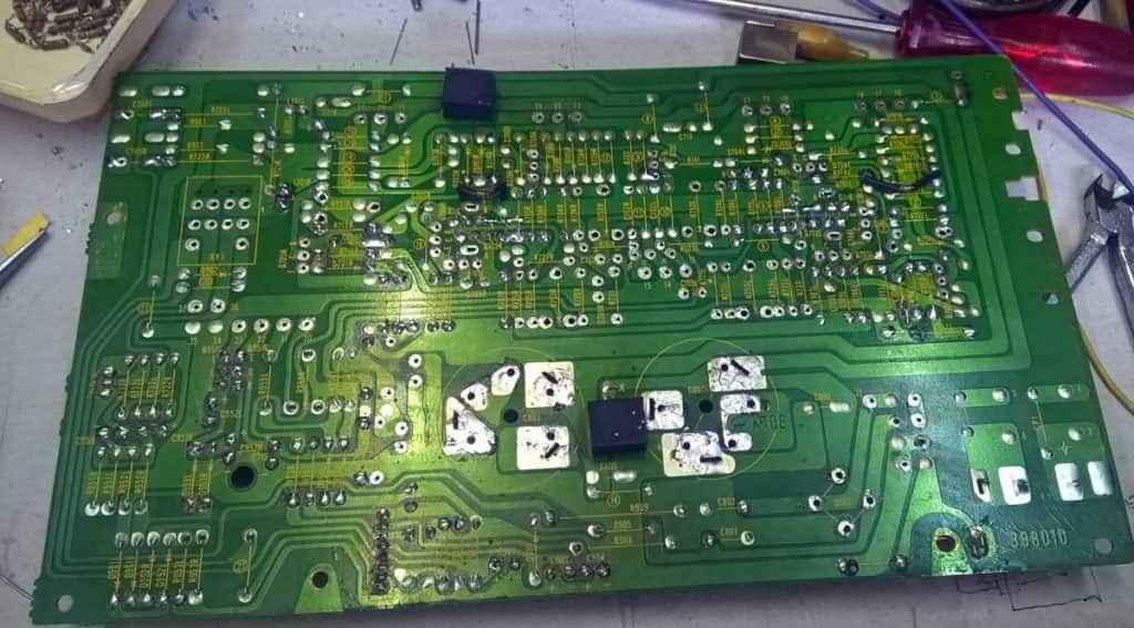
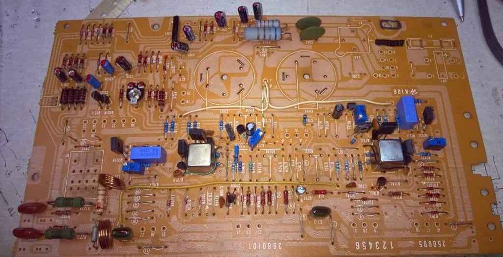
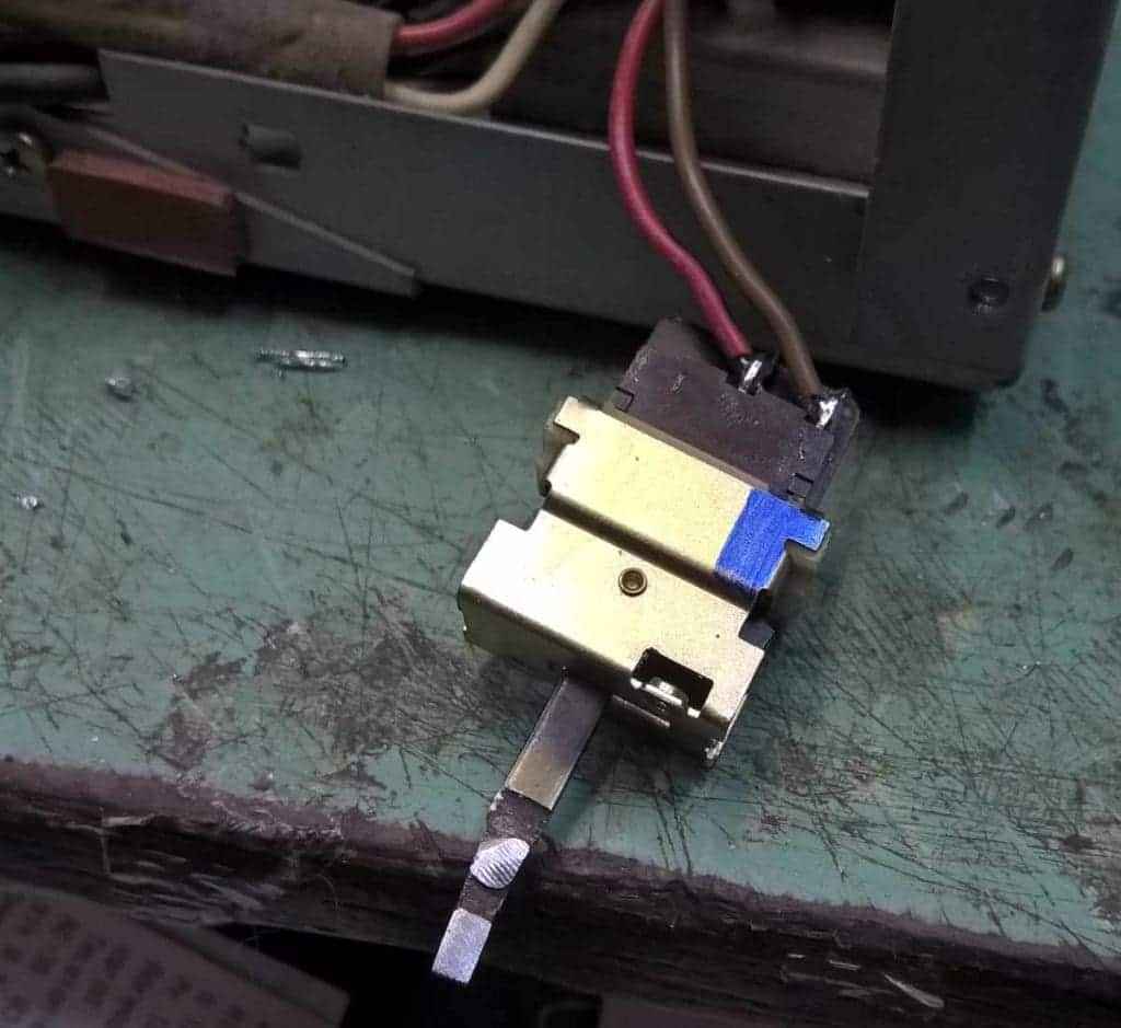
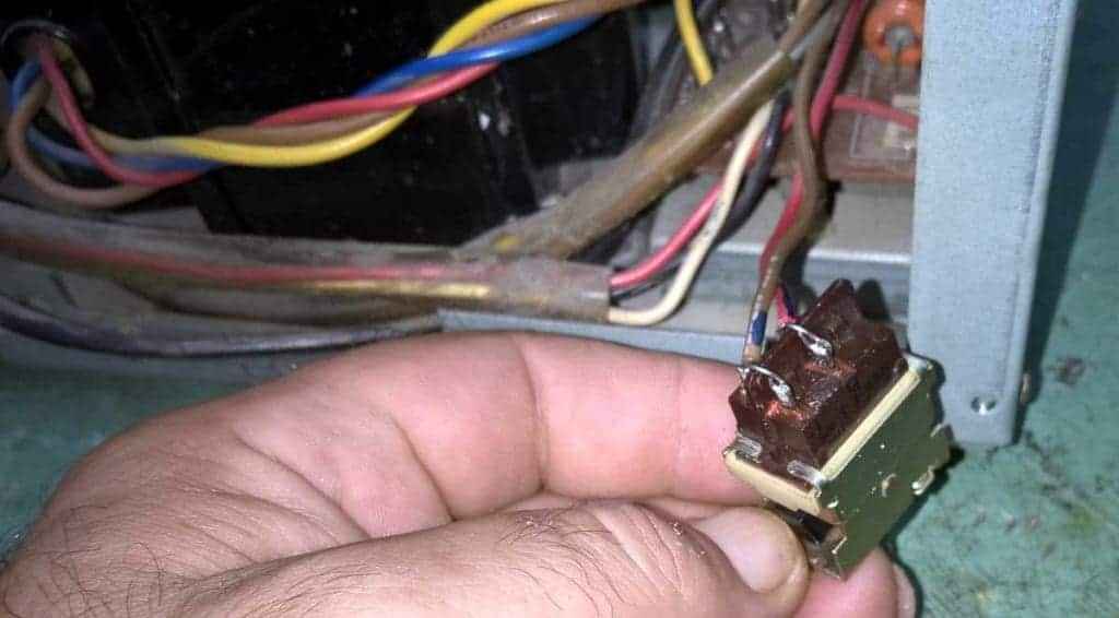
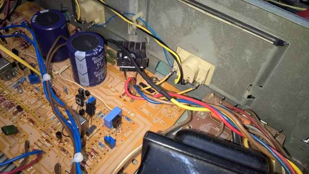
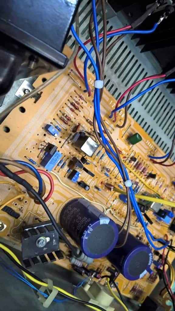
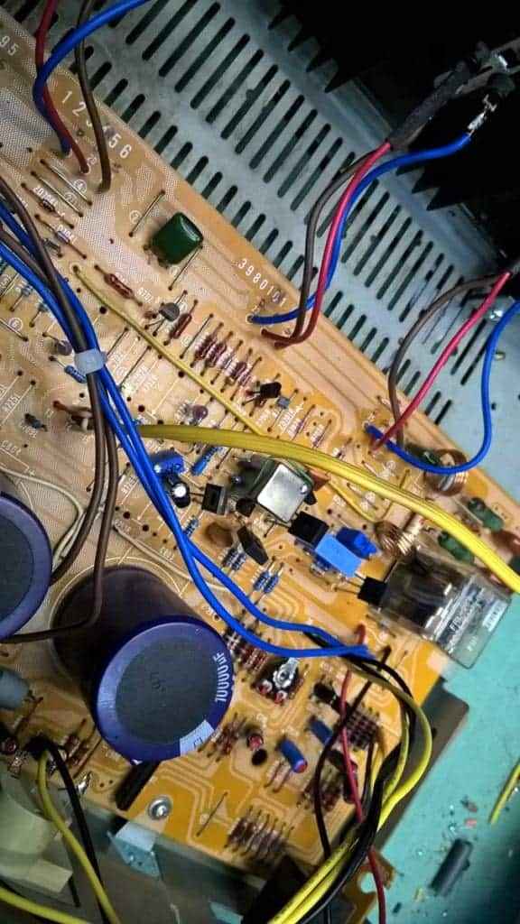
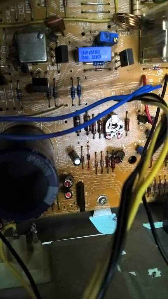
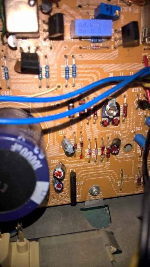
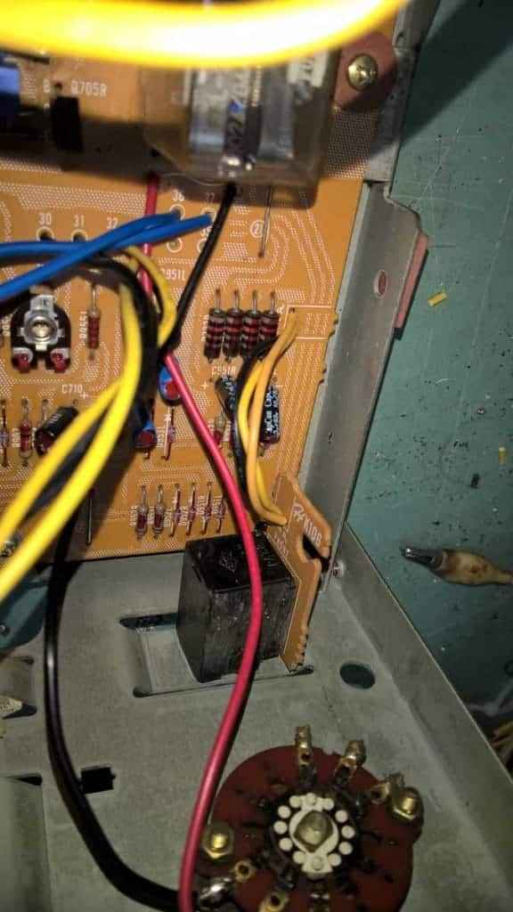
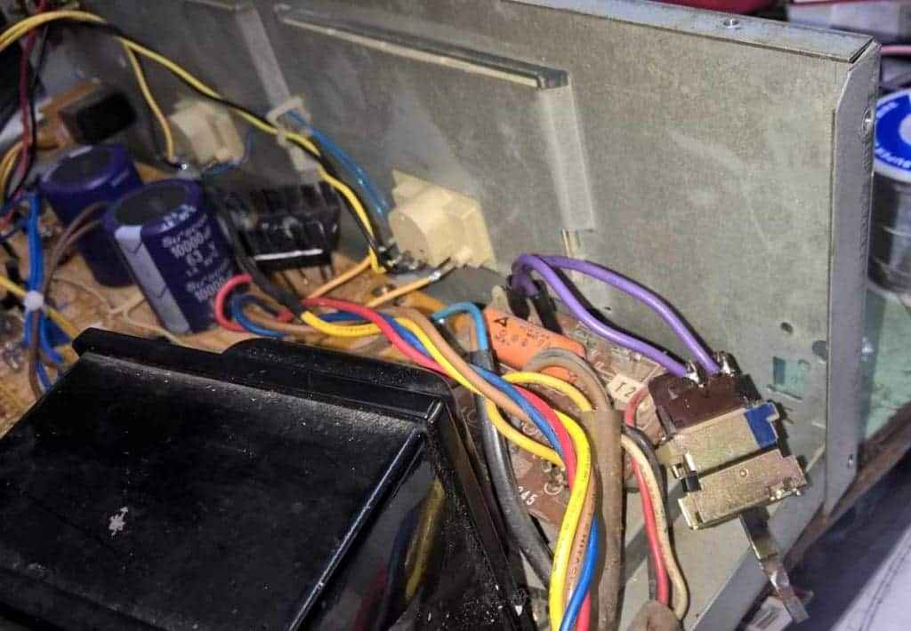
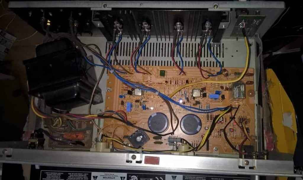
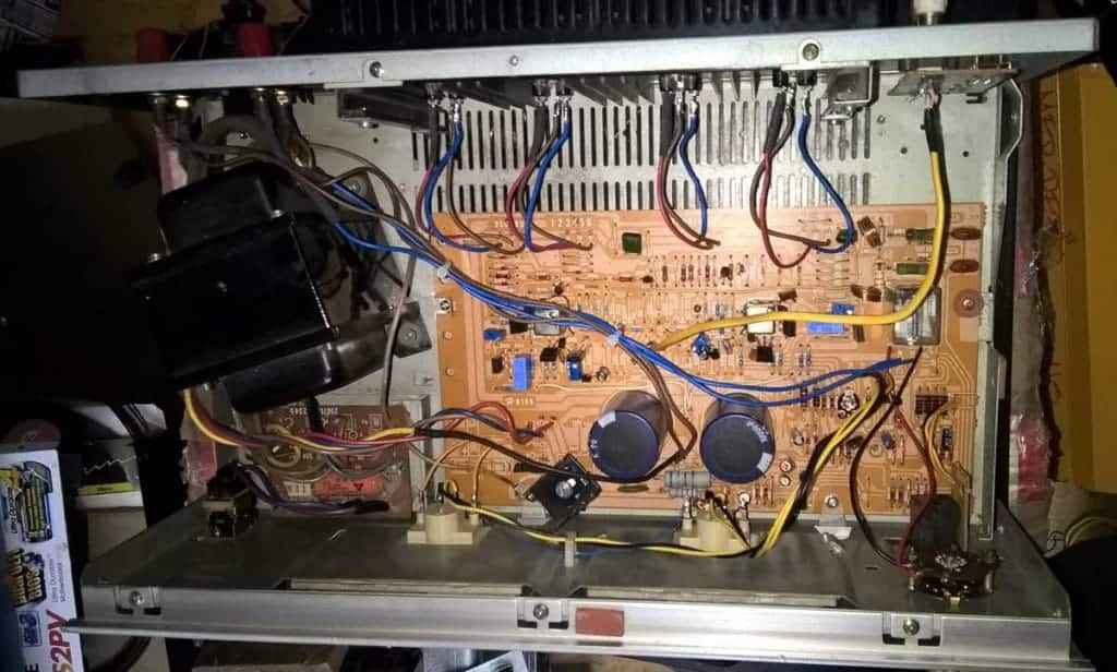
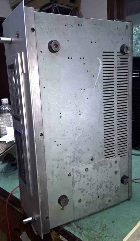
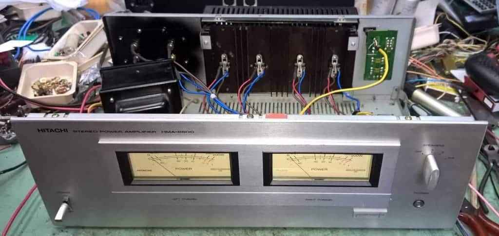
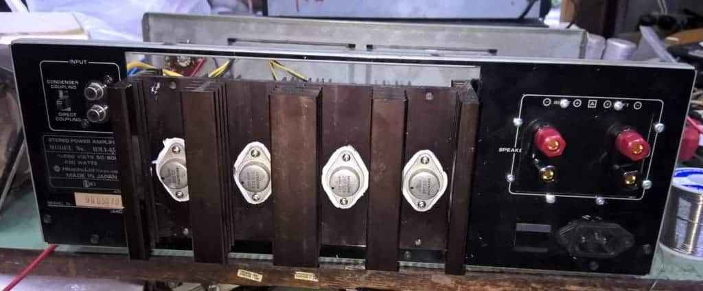
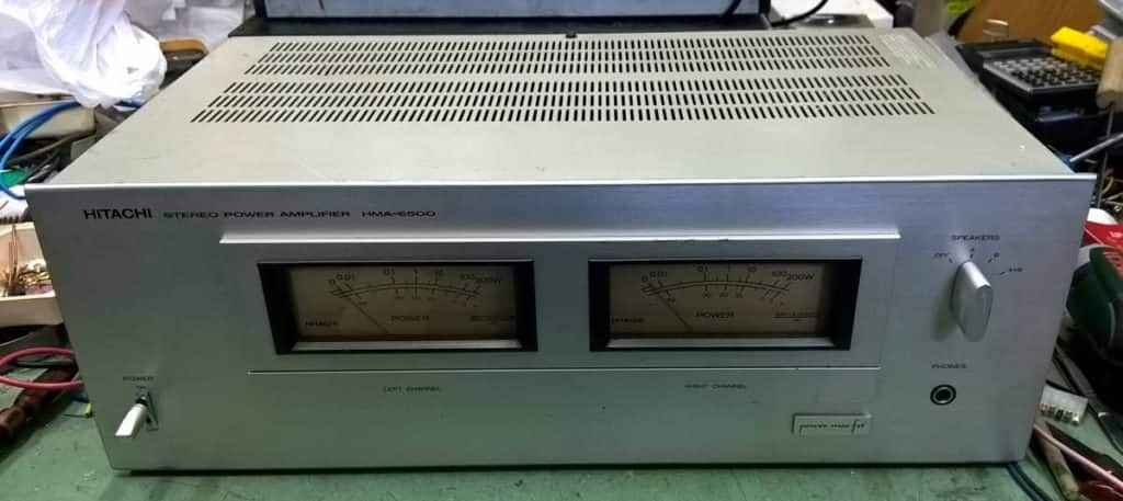
Now , let’s see what’s inside :
…. and let start diggin’ :
Plan was to make this :
…. in words , that would be :
-pull red marker and mark all parts in protection circuit and VU meters circuit , to leave them intact
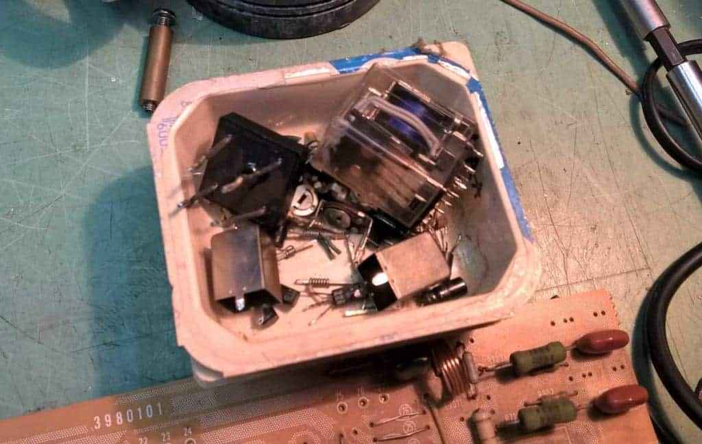
-toss out of pcb everything else ;
-wash pcb – soft brush,water,mild dish soap
-taking care of original parts nomenclature and position , where applicable , put all metal film resistors , cascoded JFet FE , MJE bjt critters instead of small 2SA/SC ones , change what’s for changing
-leave input RCAs (decent quality , minimal contact mass , which is good) , make them floating
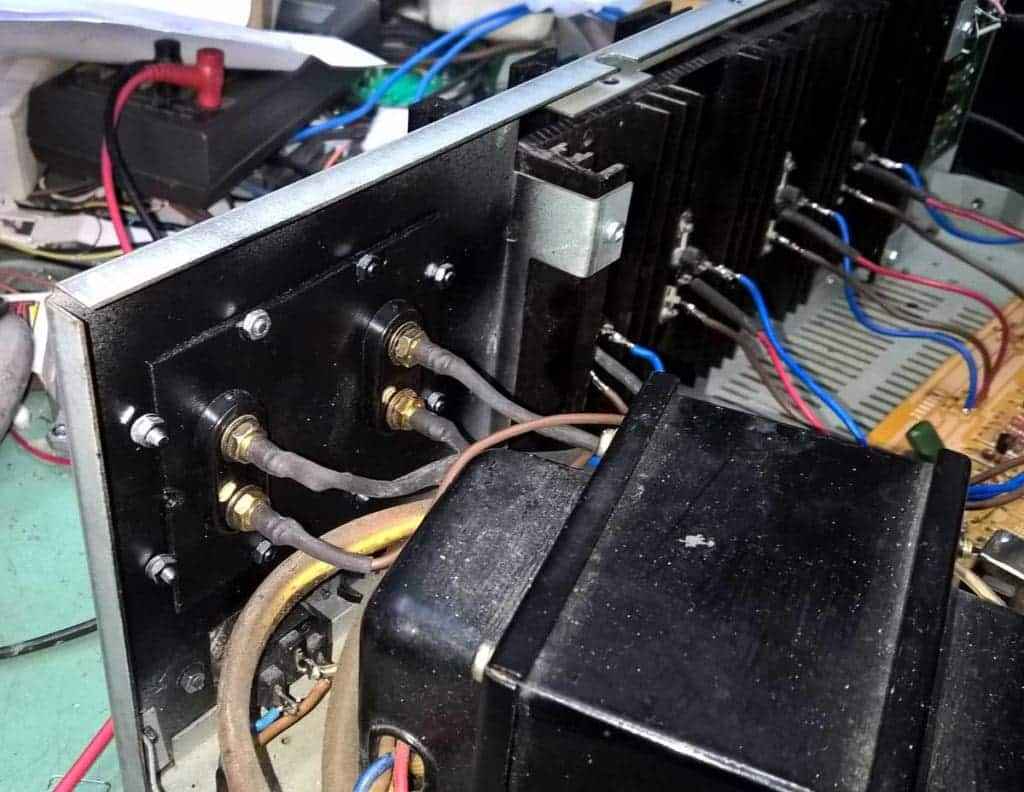
-replace output posts
-put some goop and heatsink on Graetz bridge
-drill hole to mount mains IEC inlet , connect chassis to safety GND
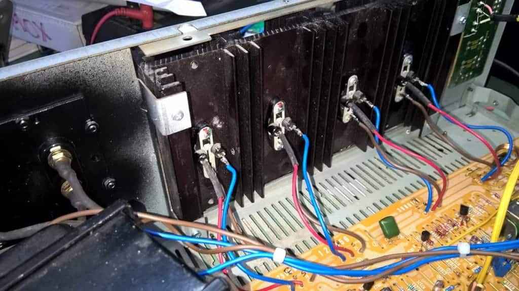
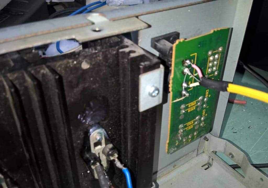
-remove old and put new mica & goop output mosfet’s interface
-open it and clean output relay contacts (ultragigamega fine sand paper)
-clean chassis inside
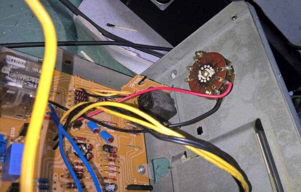
-repair power switch stud ; obviously broken in past time , someone spot-welded it , but it’s now too long and wide ; while at it , put in parallel unused section, with one in use
-existing speaker sections switch – put in series with relay coil , to function as simple speaker On/Off switch ; obviously no more A/B
-Input JFets don’t need to be scarce 2SK170BL ; you can use J309 or J310 (even SMD iteration of these , cheaper and easier to obtain) , BF862 , or any other decent JFet in that Idss and xconductance range . Boyz at Big DiyA are having Linear Systems LSK170B in Store .
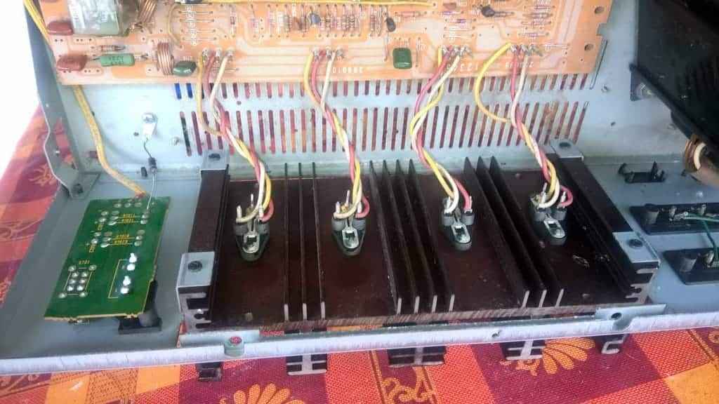
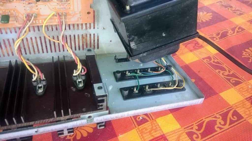
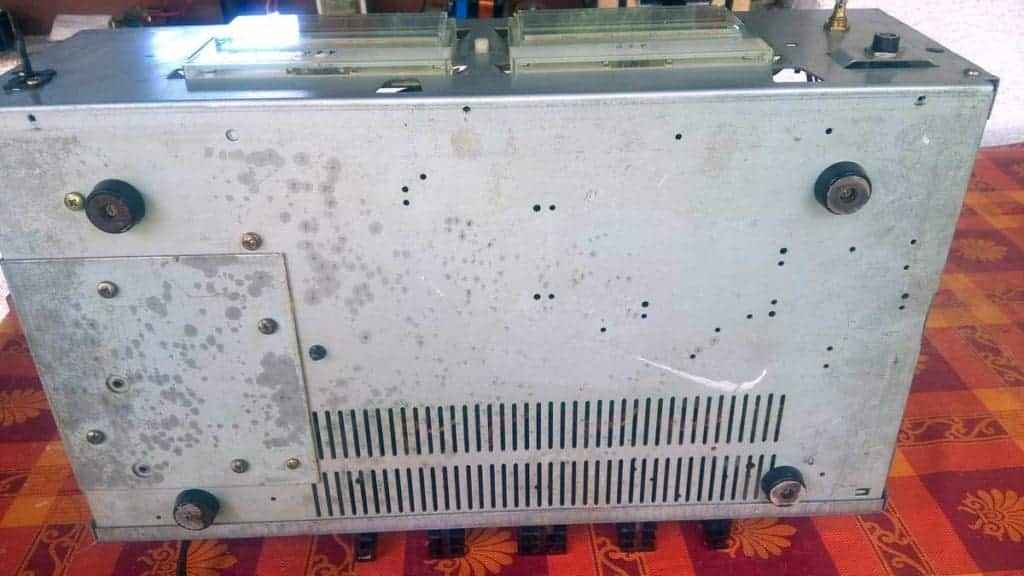
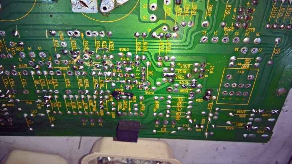
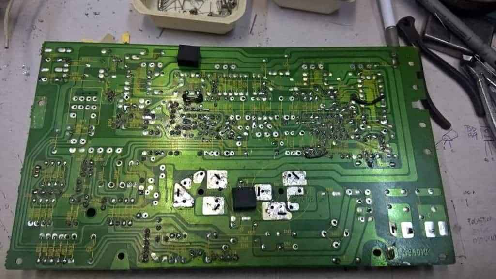
Ok , zillion pictures , as I took them :
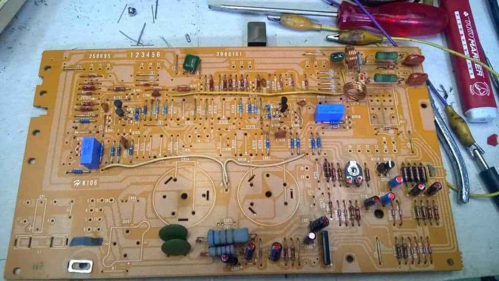
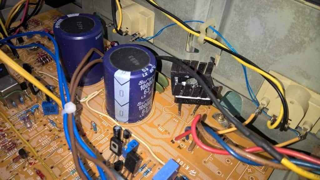
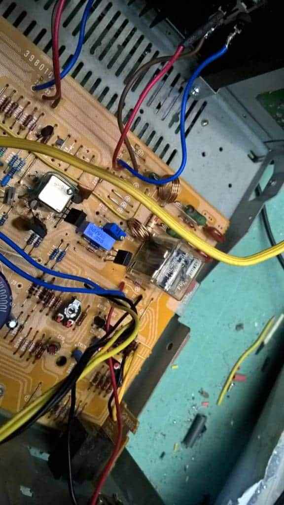
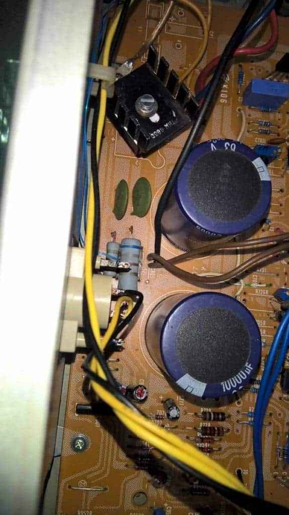
Now , absolutely crucial change to pcb traces , even if you’re not going to do any other change to circuit itself …… ; observe this :
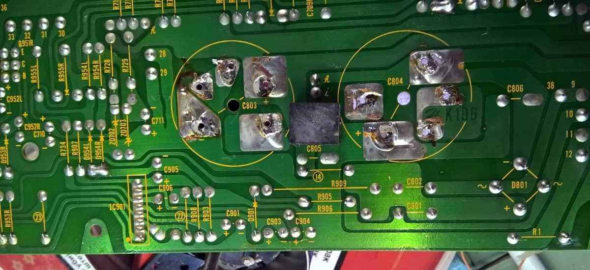
Xformer secondary is connected to (right side of pcb , down) Graetz bridge – Pt9 and Pt10 ; Pt11 and Pt12 are for center tap.
Obviously , fat trace Pt11/12 is carrying pulsating main caps charge currents, and it need to be isolated from rest of circuit …… meaning – mid point between caps need to be central ground point. However , you can see that C11 and Pt29/29 (left of left big cap place) are obviously connected to GND in easiest , not proper way , resulting in noisy (100Hz) output and tendency of oscillation of entire amp . In tech slang – GND is dirty.
So , make it like this – with exacto knife or Dremmel , cut trace where yellow ring is , and where red circle is – increase two existing holes and make new one. THAT is (red circle) new central GND point , two holes are for two loudsp GND wires (to output posts).
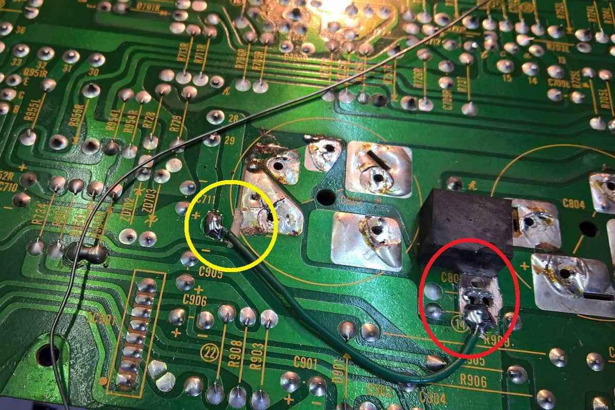
Now – relocate yellow (center tap) xformer wire from Pt10/11 , extend it with 10cm of same wire and solder in (newly drilled) third hole at central GND point .
Solder wire bridge to connect again rest of amp to GND , now in proper place …… visible on picture between yellow and red circles.
Result – amp is now dead silent in loudspeakers , without signal ; no tendency of oscillation , which is (now , when I made some extended search on net) pretty much the case even with amp not tired of years of (ab)use .
Frankly – I had some amount of headache , with my new circuit oscillating , simply because I forgot to make that change prior to everything else . Bummer is – I did spot that almost instantly after tear-down of pcb , but forgot later … which cost me several hours of time , trying to cure drek on CRO screen …
While you at there – replace R1 (bellow Graetz bridge,see pics) with CL60 or similar NTC, to properly connect audio GND and chassis.
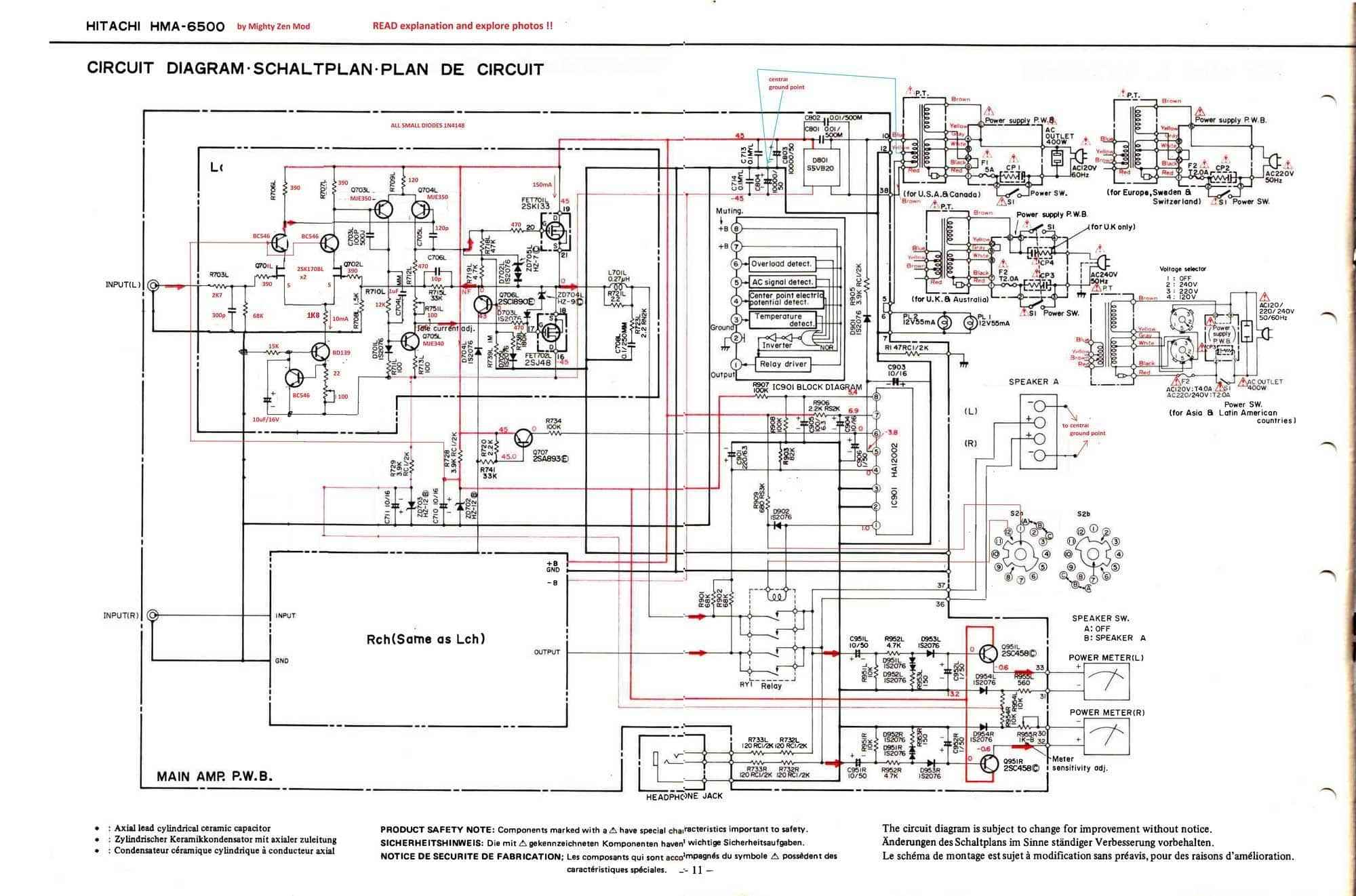
And , now , here is factory schmtc , edited , hopefully with everything what’s changed :
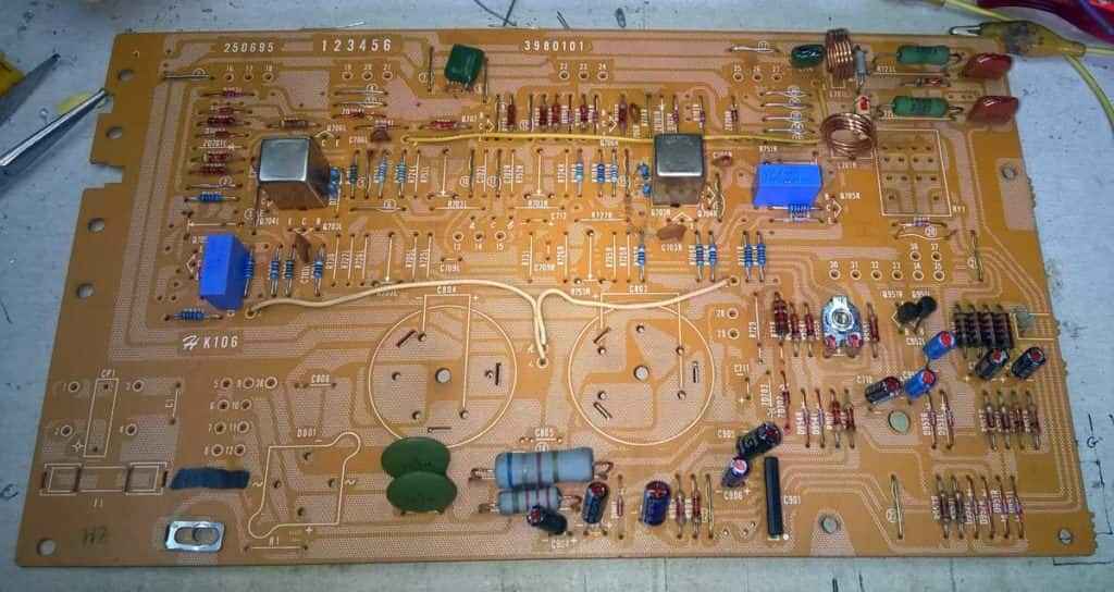
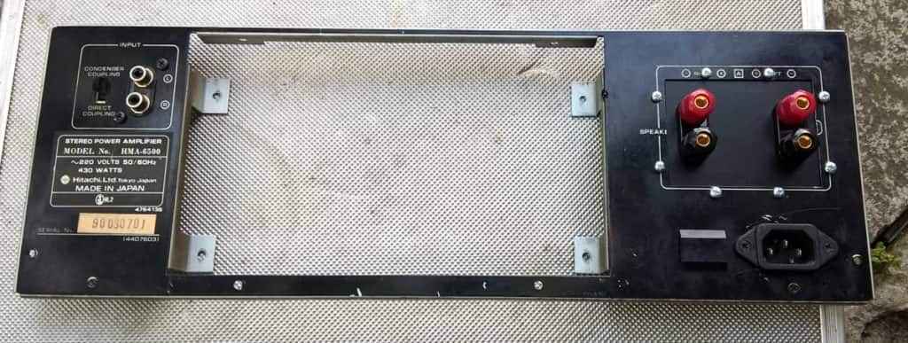
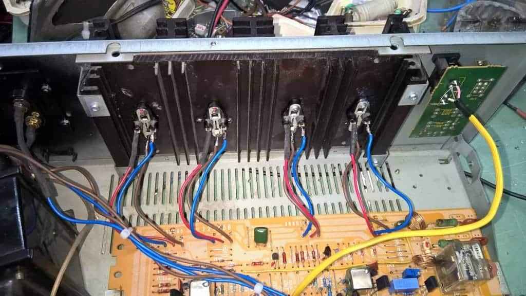
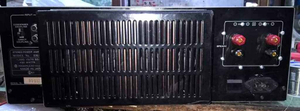
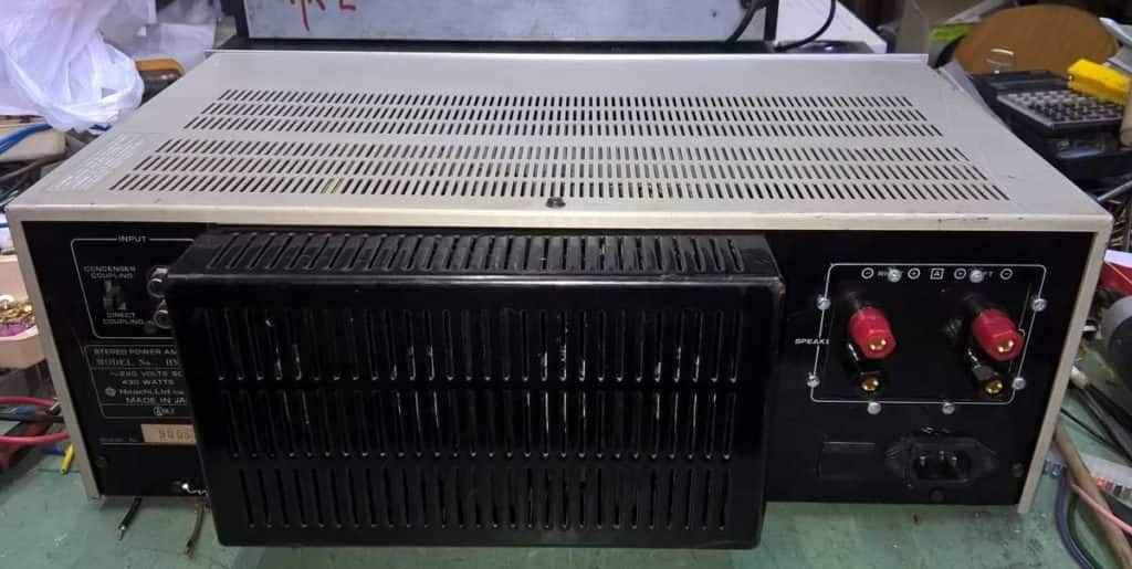
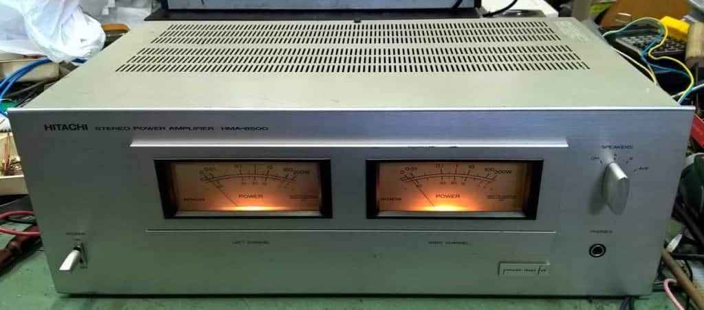
And amp (guts and outside) now looking as this :
and happy amp in action ….
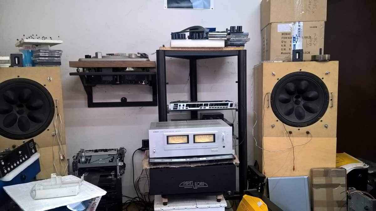
… cruising between 50 and 100mW all day long , while I was listening radio in my workshop , and peaking around 1W , when I was in da mood for da blast ; observe that my spks are 16 Ohms , so real power level is ooomphteentht lower 😉
Yup – Iq stays as from factory , 150mA ; neither heatsinks nor rest of amp could cope with more . Who prefers more , needs to make it from scratch – bigger xformer , PSU , heatsink , proper channel pcbs .
